
The amorphous silicon active readout matrix
The development of LCD (liquid crystal display) technology for the consumer market as a replacement for monitors based on cathode ray tubes, has made a technology available whose characteristics are also ideally suited for sensors in medical X-ray imaging. It is based on hydrogenated amorphous silicon (a-Si:H) which can be deposited as thin films. Amorphous silicon combines several favorable characteristics. First, it exhibits all of the semiconductor properties such as doping, photoconductivity or junction formation. This makes it suitable for the manufacture of electrical components such as TFTs (thin-film transistors) and photo diodes. Second, the plasma deposition process permits large-area deposition which allows to produce active matrices of several million pixels (Fig. 1) and sizes exceeding 40×40 cm2. Third, amorphous silicon has proven to be highly radiation hard, making it suitable for applications in medical X-ray imaging. These active matrices are the central components of flat detectors.
![]()
Fig. 1 Schematic view of the pixel structure of an indirect converting amorphous silicon active-matrix sensor array showing photodiode, TFT, as well as gate, bias and data lines
Two different conversion processes of X-ray radiation into electric charge prevail. The first approach is based on an indirect conversion process, where the X-ray radiation is converted into light which in turn is absorbed, creating electric charge. The second approach features the direct conversion of X-ray quanta into electric charge. Both methods are described in the following sections.
Flat detectors based on an indirect conversion process
The most widely used design of flat detectors as of today is based on a two-level, indirect conversion process. The X-ray quantum is absorbed creating a high energy electron via photo absorption (Fig. 2). While losing energy in the scintillator material, the electron creates a large number of electron-hole pairs which in turn recombine to produce photons in the visible range. Subsequently, this light hits the photodiode where it is converted to electric charge. This two-step conversion process has the advantage that both stages can be optimized relatively independently of one another. Figure 3 shows a schematic view of such a detector, described in detail in the following paragraphs.
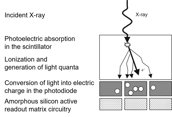
Fig. 2 Schematics of the indirect conversion process
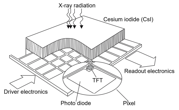
Fig. 3 Schematic view of an indirect converting flat detector based on CsI and an amorphous silicon active readout matrix
The most commonly used scintillators are gadolinium oxysulfide (Gd2O2S) and thallium-doped cesium iodide (CsI:Tl)-CsI being the scintillator of choice. CsI can be grown as needle-shaped crystals measuring 5-10 μm in diameter. This needle-shaped structure acts as a light-guide and ensures that the light—emitted in the green part of the visible spectrum—reaches the photodiode with only little scatter. The other important feature of CsI is its very good X-ray absorption property (Fig. 4), related to the high atomic numbers of Z=55 and Z=53 for cesium and iodide, respectively. It is particularly suitable for applications in general radiography, angiography and fluoroscopy which require to cover a wide range of peak voltages from 45 kVp to 120 kVp. With an effective density of 3.6 g/cm3, a CsI thickness of about 600 μm is typical for this range of applications. Even though CsI exhibits absorption minima near the K-edges around 35 keV (Fig. 4), CsI is also an adequate choice for flat detectors in mammography. Mammographic spectra, with typical peak voltages of between 25 and 30 kVp are dominated by the characteristic lines of the tube anode material (e.g. Kα at 17.5 keVand Kβ at 19.6 keV for the commonly used molebdynum), well below the K-edges of CsI. A CsI thickness of about 150 μm is typical for that application and complies with the demand for good absorption and high resolution.

Fig. 4 Absorption coefficients of CsI, a-Se and Gd2O2S as a function of X-ray photon energy
The photodiode is designed to reach a high quantum efficiency in the green part of the visible spectrum to match the spectrum of the scintillation light. Furthermore, it is optimized for high geometric aperture. At a pixel size of about 150 μm, the photodiode covers approximately 70% of the pixel area (geometric fill-factor) with current designs. Since the photons are subject to scatter processes in the CsI, however, the largest part of the signal is detected in the photodiode, no matter where the X-ray was absorbed in the continuous CsI layer in the first place. Therefore, one often refers to an effective fill-factor of 100% for all practical purposes. Taking all effects into account, an absorbed X-ray quantum with an energy of 60 keV generates a signal of approximately one thousand electrons.
The electric circuit for a TFT-based pixel structure is shown in Fig. 5. Its readout principle works as follows. First the photodiode, which acts as a capacitor, is charged to the full bias voltage prior to X-ray radiation with the TFT in its off-state. During X-ray radiation the converted optical photons are absorbed in the photodiode creating electron-hole pairs which drift to opposite contacts and gradually discharge the photodiode. The readout is initiated when the TFT is switched on via the gate line. It causes charge to flow to the photodiode so that its contact is restored to the data line voltage. The charge flow is measured in the external readout electronics and recorded as the signal. Since this step resets the photodiode to the full bias voltage the pixel is ready for the next acquisition.
![]()
Fig. 5 Pixel circuit of an active matrix with photo diode and TFT switch for data readout
The readout is performed row by row and addresses all pixels in the respective row simultaneously. Optimized low noise electronic circuits with high bandwidth are used to measure the charge and amplify the signal. These specifically designed chips may be connected to 120 or more individual readout channels. The readout chip also serves the function of a multiplexer which feeds the signals to an ADC (analog-to-digital converter). At this stage the signal is available for further processing in the image processing chain.
Flat detectors based on a direct conversion process
The direct detection process is depicted in Fig. 6. An X-ray which is absorbed in the photoconductor material generates a high energy electron. On its way through the material this electron creates many electron-hole pairs while losing its energy. An electric field is applied across the detection material to collect the generated charge carriers.
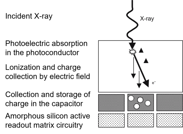
Fig. 6 Schematics of the direct conversion process
The following basic characteristics should be met by a material to qualify for a suitable direct converter: (1) high X-ray absorption, (2) large number of charge carrier generation per absorbed X-ray, (3) high collection efficiency of the charge carriers, and (4) low dark current. Photoconductor materials with a high atomic number and density and therefore good absorption characteristics, as, for example, lead iodide, lead oxide, cadmium telluride and mercury iodide are subject to current research. The best understood and most frequently used material is, however, amorphous selenium (a-Se). It can be deposited directly onto an active matrix of amorphous silicon, where each pixel consists of an electrode and a TFT.
Due to its low lying K-edge (Fig. 4), a-Se is particularly well suited for X-ray spectra used in mammography. An a-Se layer thickness of about 250 μm is sufficient for this application. For general radiography and even more so for fluoroscopy, however, adequate absorption can only be reached with an a-Se thickness of up to 1000 μm due to its relatively low atomic number (Z=34). One absorbed X-ray creates up to a thousand electron-hole pairs. By means of an applied electric field the electric charges are transported to the respective electrodes. On their way through the material to the storage electrode of the pixel, part of the generated charge is lost by recombination or deep trapping. To obtain high charge collection efficiency, field strengths of about 10 V/μm are needed which requires high voltages of approximately 10 kV applied across a 1000 μm thick a-Se layer. This in turn demands special care in the pixel design to protect the TFT from being damaged by high voltage discharge. A favorable ratio between drift length and diffusion length ensures that the charge which reaches the electrode is almost completely collected by the pixel located below the position where the X-ray quantum was initially absorbed.
The charge readout is accomplished by addressing the TFTs line by line, recharging the electrodes via the data line and measuring the respective signal in the peripheral low-noise readout electronics. The amplified signals are sequentially converted to digital signals via one or more ADCs. The signal is then fed to the image processing chain for further processing.